Electric car charger circuit diagram pdf
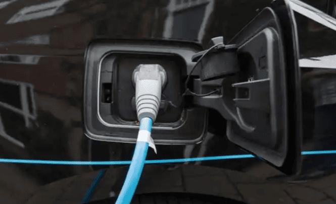
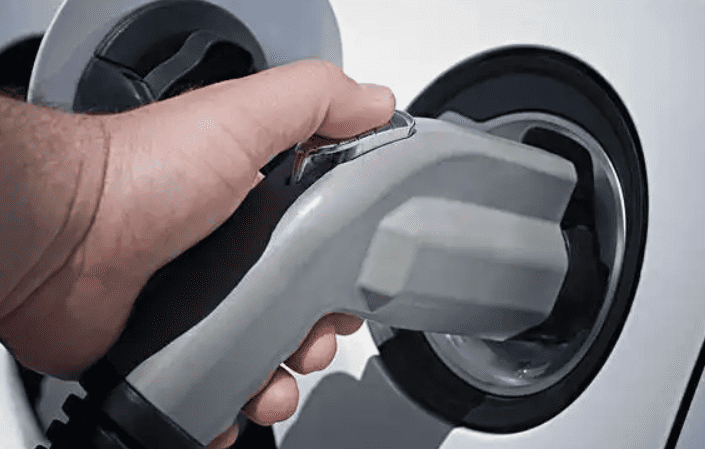
Electric car charger circuit diagram pdf: From AC to Safe DC Charging
This article provides a detailed explanation of a typical electric car charger circuit diagram, breaking down its key components and functions within the power input, conversion, control, and protection stages. Understanding this diagram is crucial for grasping how an EV charger safely and efficiently transforms grid electricity into the direct current (DC) needed to recharge a vehicle’s high-voltage battery pack. The core process involves converting alternating current (AC) from your wall outlet into stable, regulated DC, all while meticulously managing power levels and implementing robust safety mechanisms to protect both the vehicle’s expensive battery and the charger itself.
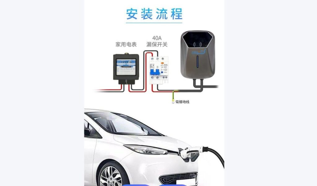
The journey of electricity begins at the input power processing stage. This is where the charger connects to the mains supply, typically a 220V AC outlet in many regions. Right at the entrance stands the Fuse, a critical sentinel for overcurrent protection. Think of it as a deliberate weak link carefully calibrated to the circuit’s maximum safe current. If an unexpected surge or internal fault causes the current to exceed this rating – perhaps due to a short circuit or component failure – the thin metal wire inside the fuse heats up rapidly and melts (blows), physically breaking the circuit connection. This swift action instantly cuts off the incoming power, preventing potentially catastrophic damage to downstream, more expensive components like transformers or control chips. Following the fuse is the Bidirectional EMI Filter (like component T0). This network, constructed from inductors (which resist changes in current) and capacitors (which resist changes in voltage), acts like a sophisticated noise barrier. It performs two vital functions: firstly, it prevents high-frequency electrical “noise” or interference present on the incoming mains power – generated by other appliances, industrial equipment, or even lightning – from entering the charger’s sensitive internal electronics and causing malfunctions or erratic behavior. Secondly, it equally prevents the high-frequency switching noise inevitably generated inside the charger itself (primarily by the rapidly switching MOSFET later on) from leaking back onto the household or public power grid, where it could interfere with other electronic devices or violate electromagnetic compatibility (EMC) regulations. Next in line are the Rectifier Diodes (D1-D4), usually arranged in a classic bridge configuration. These semiconductor devices act like one-way electrical valves. Their specific arrangement allows them to flip the negative half-cycles of the incoming AC sine wave into positive cycles. The result is not yet smooth DC, but rather a pulsating DC voltage that rises and falls significantly. To smooth out these harsh pulsations, the Filter Capacitor (C11) comes into play. This large capacitor acts like an electrical reservoir or buffer. During the voltage peaks from the rectifier, it charges up, storing electrical energy. During the dips between peaks, it discharges, supplying power to the circuit. This charging and discharging action significantly reduces the voltage ripple, transforming the pulsating DC into a much smoother, relatively stable high-voltage DC level – typically around 300V DC when rectifying 220V AC. This high-voltage DC bus serves as the primary energy source for the next critical stage: power conversion.
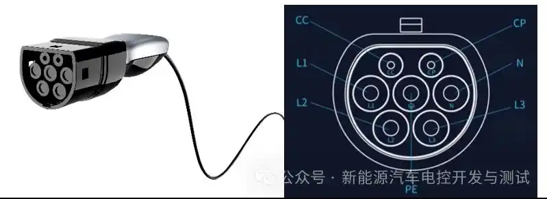
The heart of the charger’s operation lies in the power conversion section, where high-voltage DC is efficiently transformed into the precise voltage and current needed by the EV battery. This task is orchestrated by the Pulse Width Modulation (PWM) Integrated Circuit (like the TL3842). This specialized control chip is the brain of the charger. It requires power to operate, supplied between its positive supply pin (pin 7) and ground (pin 5). Its core function is generating a precisely timed stream of high-frequency pulses at its output pin (pin 6). The width (duration) of these pulses is constantly adjusted based on feedback signals. Pin 4 is connected to an external timing resistor (R1) and capacitor (C1) – these components form an oscillator circuit whose values directly determine the fundamental switching frequency (often tens or hundreds of kilohertz) of the PWM IC. This frequency significantly impacts the size of magnetics (like the transformer) and the overall efficiency of the power conversion. Pin 3 is the Current Limit Pin. By connecting an external resistor to this pin and ground, engineers can program the charger’s maximum allowable output current. If the sensed current tries to exceed this preset limit, the PWM IC automatically reduces the pulse width to clamp the current. Pin 2 is the Voltage Feedback Pin. This is where information about the actual output voltage (sensed later in the circuit) is fed back. The chip continuously compares this feedback voltage against an extremely stable internal reference voltage. If the output voltage is too low, the chip increases the pulse width; if it’s too high, it decreases the width. This constant adjustment loop ensures the output voltage remains rock-solid at the desired level, regardless of fluctuations in the input voltage or changes in the battery’s state of charge. The pulses generated by the PWM IC’s pin 6 directly drive the gate of the Metal-Oxide-Semiconductor Field-Effect Transistor (MOSFET) (Q1, e.g., K1358). This powerful transistor acts as a high-speed electronic switch. When the PWM pulse is “high,” the MOSFET turns fully on, allowing the high-voltage DC (around 300V) to flow through its drain and source, and consequently through the primary winding of the High-Frequency Pulse Transformer (T1). When the PWM pulse is “low,” the MOSFET switches off instantly, stopping the current flow. This rapid on-off switching effectively chops the high-voltage DC into a high-frequency square wave AC flowing through the transformer primary. The transformer itself performs two crucial functions: Isolation and Voltage Transformation. Its primary and secondary windings are physically separated by insulation, creating a vital safety barrier that prevents any direct electrical connection between the potentially lethal high-voltage primary side (connected to the mains) and the low-voltage secondary side (connected to the vehicle battery). Simultaneously, it steps down the high-voltage AC on its primary side to a much lower AC voltage on its secondary side, suitable for battery charging (e.g., converting 300V DC chopped to AC down to maybe 50V AC). Crucially, additional windings on the transformer are often used to generate auxiliary power supplies (like +12V or +15V) needed to run the PWM IC itself and other control logic, eliminating the need for a separate power brick. The low-voltage AC emerging from the secondary winding must now be converted back to DC. This is the job of the High-Frequency Rectifier Diode (D4). Unlike standard mains frequency diodes, this diode is specifically designed to handle the very rapid switching transitions (fast recovery time) and high frequencies involved. It rectifies the secondary AC, allowing current to flow only towards the battery. Finally, the Low-Voltage Filter Capacitor (C10) smoothes the rectified output. While the secondary voltage is much lower than the primary, the rectification process still creates pulsations. Capacitor C10 absorbs these ripples, charging during the voltage peaks and discharging during the troughs, resulting in a much smoother and stable DC voltage ready to be fed to the battery terminals.
Precision control over the charging voltage and current is paramount, handled by dedicated feedback and setting circuits. As mentioned, the Voltage Feedback Pin (Pin 2 of the PWM IC) is the linchpin for output voltage regulation. The actual voltage delivered to the battery is constantly monitored, usually via a precision resistor divider network connected across the output terminals. This scaled-down voltage signal, representing the true output voltage, is fed back to pin 2. Inside the PWM IC, a sophisticated error amplifier continuously compares this feedback voltage to its ultra-stable internal reference voltage (e.g., 2.5V). Any difference between these two voltages generates an “error” signal. This error signal directly influences the width of the pulses generated at pin 6. If the output voltage starts to sag (perhaps because the battery is accepting more current), the error signal tells the PWM IC to increase the pulse width. Wider pulses mean the MOSFET conducts for a longer fraction of each cycle, allowing more energy transfer through the transformer, thereby boosting the output voltage back to its setpoint. Conversely, if the output voltage rises too high, the error signal triggers narrower pulses, reducing energy transfer and lowering the voltage. This closed-loop feedback system operates continuously and rapidly, ensuring the output voltage remains exceptionally stable. Equally critical is limiting the maximum current delivered to the battery to prevent overheating and damage. This is managed via the Current Limit Pin (Pin 3 of the PWM IC). The charger’s maximum output current is set by the value of an external resistor connected between pin 3 and ground. Internally, the PWM IC monitors the voltage drop across a Current Sampling Resistor (R27) located in series with the charging path – typically on the secondary/low-voltage side, although sometimes inferred on the primary side. As charging current flows through R27, it creates a small but proportional voltage drop (V = I * R). This voltage is amplified and compared against a threshold set by the resistor on pin 3. If the sensed current (represented by the voltage across R27) approaches the preset maximum, the PWM IC automatically reduces the pulse width (duty cycle) at pin 6. This action limits the power transferred through the transformer, effectively capping the output current at the safe maximum level. This is crucial during the initial “constant current” phase of charging a depleted battery. The Oscillator Resistor and Capacitor (R1 and C1 connected to Pin 4) form the timing network that sets the fundamental operating frequency of the PWM IC. The values chosen for R1 and C1 determine how fast the internal oscillator runs, directly setting the switching frequency. This frequency choice involves critical trade-offs: higher frequencies allow the use of smaller, lighter transformers and filter capacitors, but can lead to increased switching losses in the MOSFET and diode, potentially reducing overall efficiency. Lower frequencies reduce switching losses but require larger magnetics. The design frequency is carefully optimized for the charger’s power rating and target efficiency.
Robust protection mechanisms are integrated throughout the circuit to safeguard against failures and ensure safe operation under all conditions. Output Over-Voltage Protection (OVP) is a critical last line of defense. While the primary voltage feedback loop is highly reliable, catastrophic failures (like the PWM IC malfunctioning, the optocoupler failing open, or the voltage feedback path being broken) could theoretically cause the output voltage to soar uncontrollably, posing a severe risk to the expensive EV battery. The OVP circuit, often utilizing a Zener Diode (D5) combined with a comparator or directly triggering a shutdown path, constantly monitors the output voltage. The Zener diode is chosen with a breakdown voltage slightly higher than the maximum normal output voltage. If the output voltage unexpectedly exceeds this Zener voltage plus a small margin, the Zener diode abruptly begins conducting heavily. This sudden conduction can either directly pull down a control signal or trigger a comparator, which then forces the PWM IC to stop switching immediately or triggers a latching shutdown circuit, completely disabling the output. This fast-acting response prevents dangerous overvoltage conditions. The Optocoupler (like 4N35) plays a dual vital role in both control and safety. It consists of an internal light-emitting diode (LED) on one side and a light-sensitive transistor (phototransistor) on the other, separated by an insulating barrier. In the voltage feedback path, the signal representing the output voltage controls the current flowing through the LED. The brightness of this LED light directly controls the conduction of the phototransistor on the primary (high-voltage) side. This allows the output voltage information to be accurately transmitted across the safety isolation barrier provided by the transformer to the PWM IC’s feedback pin (pin 2). Crucially, this optoisolation ensures no direct electrical connection exists between the potentially hazardous high-voltage primary circuit and the low-voltage secondary/battery circuit, significantly enhancing safety. The Current Sampling Resistor (R27) serves not only for current regulation but also as a key element for Over-Current Protection (OCP). While the PWM IC’s pin 3 provides programmable current limiting during normal operation, a separate, faster-acting OCP circuit often monitors the voltage across R27. If an extremely rapid surge or short circuit occurs, causing the current to spike dangerously fast – potentially faster than the main PWM control loop can respond – the OCP circuit detects this excessive voltage drop across R27 and triggers an immediate shutdown of the PWM IC or the main power switch. This rapid intervention protects components like the MOSFET, rectifier diode, and transformer from destruction due to extreme overload currents.
In conclusion, an electric car charger circuit diagram reveals a sophisticated interplay of power electronics, control theory, and stringent safety engineering. Starting with conditioning the raw AC input through filtering and rectification, it then employs high-frequency switching (controlled by a dedicated PWM IC and power MOSFET via a transformer) to efficiently step down and isolate the voltage. Meticulous feedback loops, enabled by components like the optocoupler and current sense resistor, provide precise regulation of both output voltage and current, essential for battery health. Finally, multiple overlapping protection layers – including fuses, current limiting, over-voltage shutdown, and over-current protection – ensure the system operates reliably and safely under normal conditions and fails gracefully in the event of faults. Understanding these core sections demystifies how these essential devices safely deliver the energy that powers electric transportation. When searching for an “electric car charger circuit diagram pdf,” you’ll typically find schematics detailing these interconnected stages, providing invaluable insight for design, troubleshooting, or educational purposes.
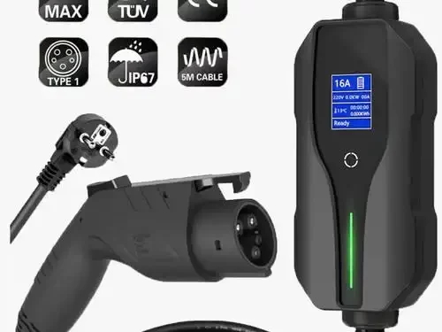
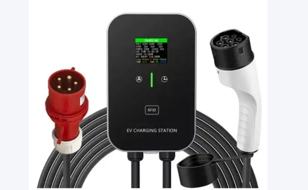
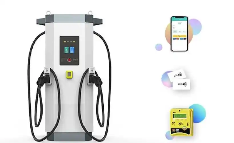
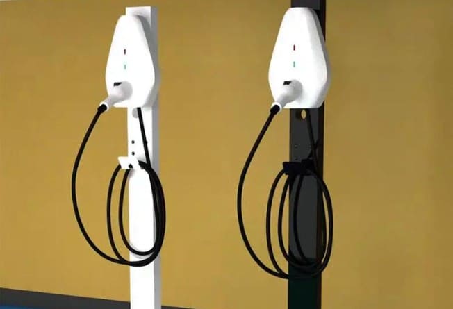
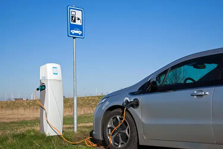
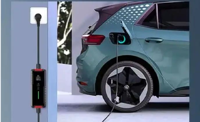
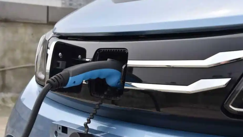
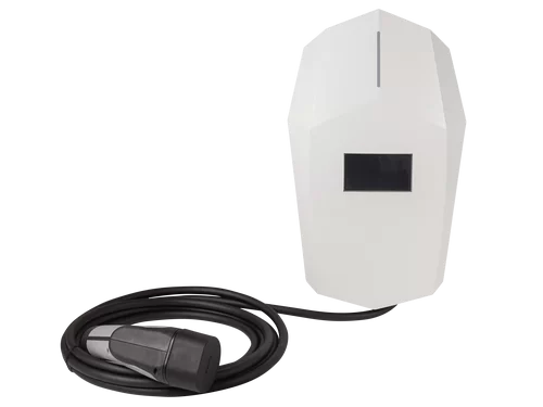
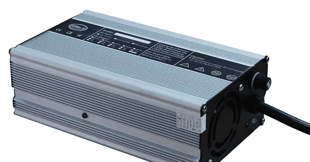
Recommend Slow Charger Products:
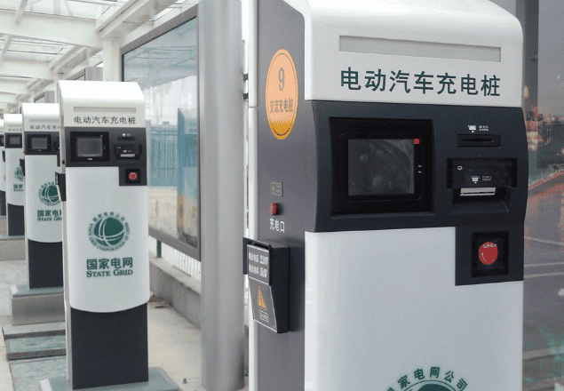
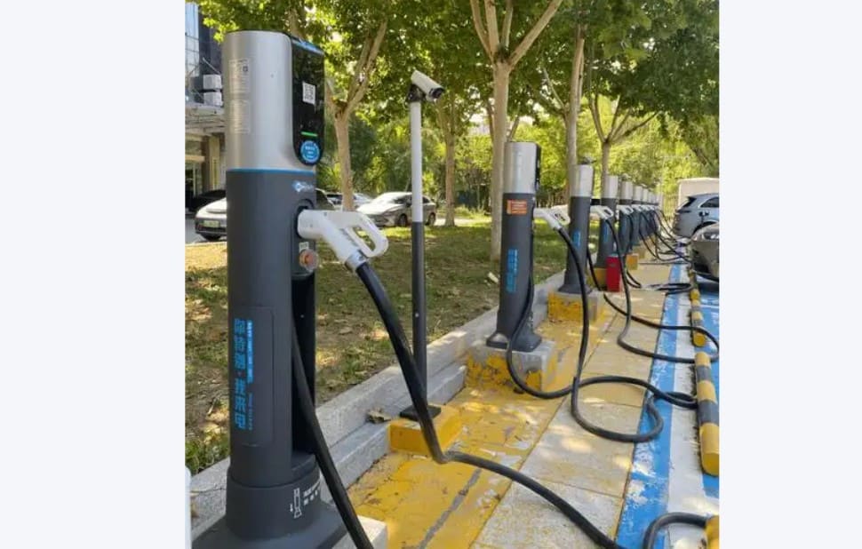
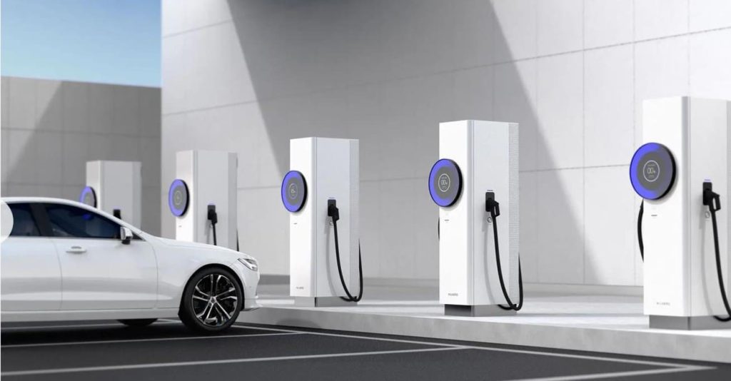
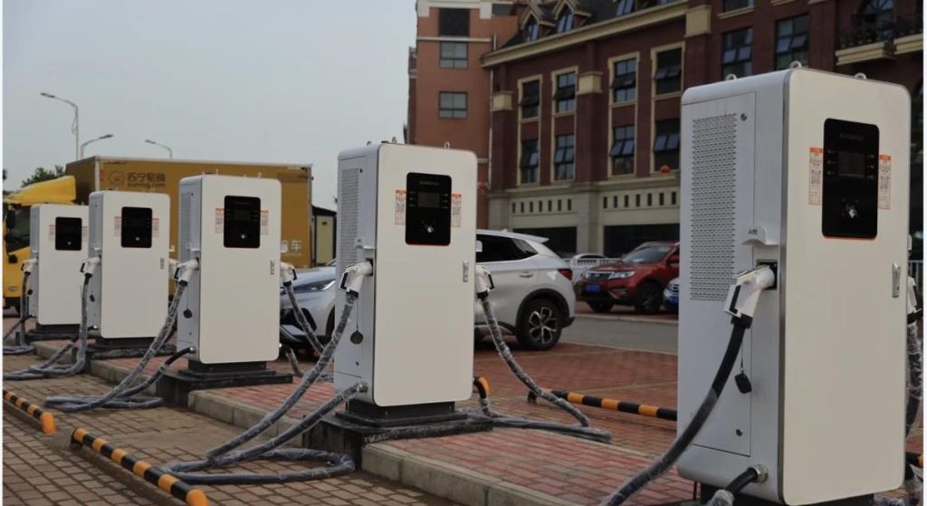
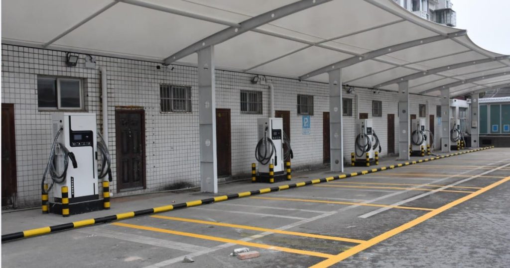
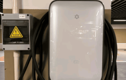
Charging pile:
Contact Us
Whatsapp/Mobile: +86 18019762979
Email: sales@lkmixer.com